Reference designs
This chapter will provide example designs for the W-Modbus module.
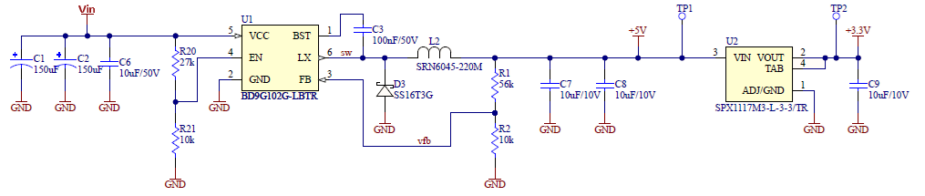
Reference design part 1 - Power supply
The following design can be used as a reference for the power supply circuitry. It employs a buck converter to regulate the input voltage to 5 V, which is then converted to 3.3 V using an LDO. The 3.3 V supply (VCC) provides power to the W-Modbus module, while the 5 V rail can be used to supply, for instance, the RS485 driver circuit.
Reference design part 2 - RS485
This section shows an example of an RS485 driver implementation. DE, TX, RX and RE are connected to the W-Modbus module as shown in part 3.
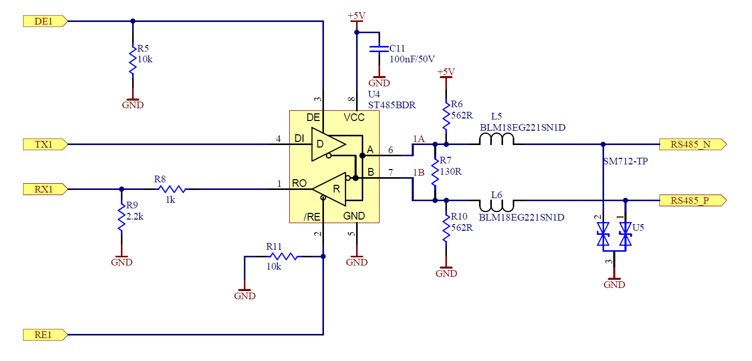
NOTE: Voltage on RX must NOT exceed 3.3 V! Since the RS485-driver (U2) is using 5 V logic levels has its RO pin (RX) connected to the Module (U1) with cmos level I/O's, a level shifting circuit (such as a resistor devider shown in the schematic) must be used!
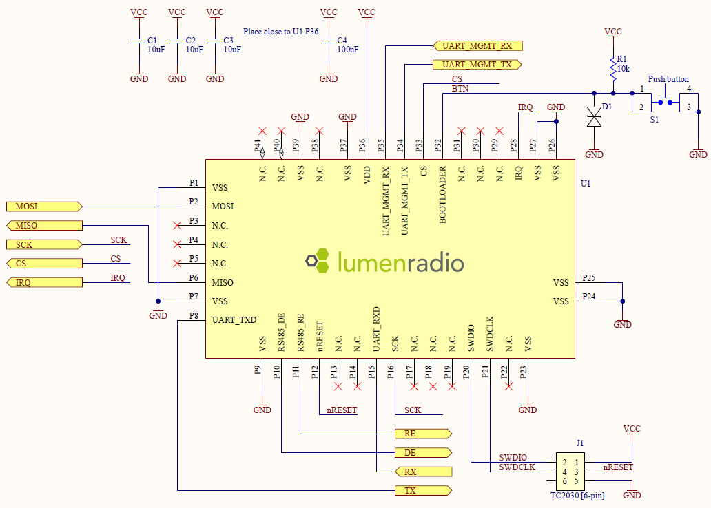
Reference design part 3 - Module
This section presents an illustration of how the W-Modbus Module and its peripherals can be connected. See Pin assignments for further description of the module pins.
Design files
Electrical and mechanical design files (symbols, footprints and 3D models) are available at the W-Modbus Module support page.