Pin Assignments and Functions
This section describes the pin assignments and pin functions.
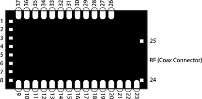
Pin assignments
Module seen from the top

Pin functions
| Pin | Name | Pin type | Description |
|---|---|---|---|
| 1 | VSS | Power | Ground (0V) |
| 2 | IRQ | Digital output | Interrupt signal, active low |
| 3 | CS | Digital input | Chip select, active low |
| 4 | SCK | Digital input | SPI clock |
| 5 | MOSI | Digital input | SPI Master Out, Slave In |
| 6 | MISO | Digital output | SPI Master In, Slave Out |
| 7 | VSS | Power | Ground (0V) |
| 8 | DMX_TXD | Digital output | DMX TXD |
| 9 | VSS | Power | Ground (0V) |
| 10 | RS485_DE | Digital output | RS485 driver control signal |
| 11 | RS485_RE | Digital output | RS485 driver control signal |
| 12 | DMX_RXD | Digital input | DMX RXD (3.3 V max) |
| 13 | RDI_LVL0 | Digital output | Radio level LED |
| 14 | RDI_LVL1 | Digital output | Radio level LED |
| 15 | RDI_LVL2 | Digital output | Radio level LED |
| 16 | RDI_LVL3 | Digital output | Radio level LED |
| 17 | RDI_LVL4 | Digital output | Radio level LED |
| 18 | RDM | Digital output | RDM LED |
| 19 | DMX | Digital output | DMX LED |
| 20 | N.C. | No connection | Do not connect |
| 21 | N.C. | No connection | Do not connect |
| 22 | VSS | Power | Ground (0V) |
| 23 | VSS | Power | Ground (0V) |
| 24 | VSS | Power | Ground (0V) |
| 25 | VSS | Power | Ground (0V) |
| 26 | VSS | Power | Ground (0V) |
| 27 | VSS | Power | Ground (0V) |
| 28 | SCL | Digital input/output | I2C clock to RGB LED driver1 |
| 29 | SDA | Digital input/output | I2C data to RGB LED driver1 |
| 30 | VSS | Power | Ground (0V) |
| 31 | N.C | No connection | Do not connect |
| 32 | LINK_SW | Digital input | Link control switch input |
| 33 | STATUS_LED | Digital output | Status LED |
| 34 | LINKED | Digital output | Linked to transmitter LED |
| 35 | RF_LINK | Digital output | RF link LED |
| 36 | VDD | Power | Power supply (3.3V) |
| 37 | VSS | Power | Ground (0V) |
| ANT | RF ANT | RF | Antenna connector |
1 Shall be pulled high (to Vcc) through a 4.7 kOhm resistor if RGB LED is used.
TimoTwo has some additional pads on the bottom layer not lined out in this table, these pads shall be left unconnected, and shall not be matched with any corresponding pads on the PCB. The PCB shall be left without any copper under the module.
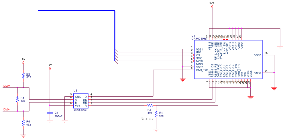
Typical Application Circuit
