Reference designs
Example: DALI interface circuitry
Show BOM list
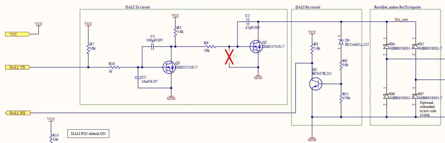
A DALI interface circuit to connect the W-DALI module to a DALI bus can be constructed as in the design above.
DALI Tx circuit: Purpose: allow device to sink the required current during DALI transmission. DALI TX offpage is connected directly to the corresponding pins of W-DALI module. R7 is used as an external pull up to keep the bus at defined inactive state if the DALI module is restarted or similar. R10, C3, and C5 are all used to trim the on and off slope of Q3 FET which acts as a signal polarity inverter. It in turn controls the gate of Q2, which is the main current sinking FET and must be able to continously sink 260mA if it is used to connect to a DALI bus according to IEC 62386. C2, R6, and R5 can all be trimmed fo adapt signal slope.
DALI Rx circuit: The purpose of this circuit is to separate W-DALI module from the high voltages of the DALI bus. It also polarity flips the signal voltage so that 3.3V at DALI_RX pin corresponds to an active bus. Q4 is operated in saturation mode and its base voltage is controlled by the R9 and R11 divider together with the D3 zener. If the DA_rect voltage is below the D3 breakdown voltage, no current will flow through the Q4 base and DALI_RX net will be pulled high. If the bus is inactive with a coltage higher than the D3 breakdown voltage, reverse current will flow through D3 and correspondingly, through R9, D11 and Q4 base. This will result in a low voltage on DALI_RX due to the current through R8 and Q4 to GND.
DA Rect: This diode bridge rectifies the DALI bus voltage. Diodes need to be dimensioned to handle the necessary current on the bus.
Show image of rise and fall times
Example: DALI PSU (simple)
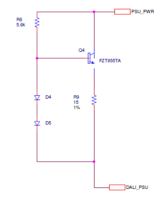
This is a simplistic but adequate low power DALI PSU circuit design. The minimum supply current for the DALI bus utilizing the above circuit is 30mA with a short circuit current of approx. 50mA. If higher supply current capabilities are required for power of a sensor from the DALI bus a more advanced DALI PSU design is required. In the circuit above the voltage drop of the base-emitter is matched by the voltage drop of diode D4. The voltage drop over D5 is therefore equal to the voltage drop of R9 which resistance will dimension the short circuit current. When the short circuit current is reached the voltage dop over R9 becomes larger than the voltage drop over D5. When this happens the two diodes will start to conduct and the current will flow through the diodes and not to the base of Q4 which then turns off.
Example: DALI PSU (precise)
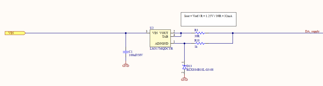
A more advanced PSU design can be achieved using the above circuit, which allow for more precise control over guaranteed PSU current while keeping the max current fairly close to the guaranteed.
The VIN pin of U2 is supplied with a constant voltage source of 17-21V. U2 tries to regulate the output voltage such that the voltage on pin 1 is 1.25V below VOUT, i.e the voltage drop over output resistance R3 shall not exceed 1.25V. If there is little current through R3 such that the drop over R3 is lower than 1.25V, the VOUT pin voltage will increase until i reaches the input rail minus dropout voltage and act as a constant voltage supply. If output current is too high, such that the voltage on pin 1 will become lower than 1.25V below VOUT, U2 will respond by lowering the output voltage and in such a way act as a current limiting circuit. Pin 1 has a high impedence input and thus the value of R18 is not critical.