Layout considerations
Electrical and mechanical design files are available for download at the support page.
Any measurement on this page is implicitly written in millimeters, if not specified otherwise.
W-DALI OEM module pad dimensions
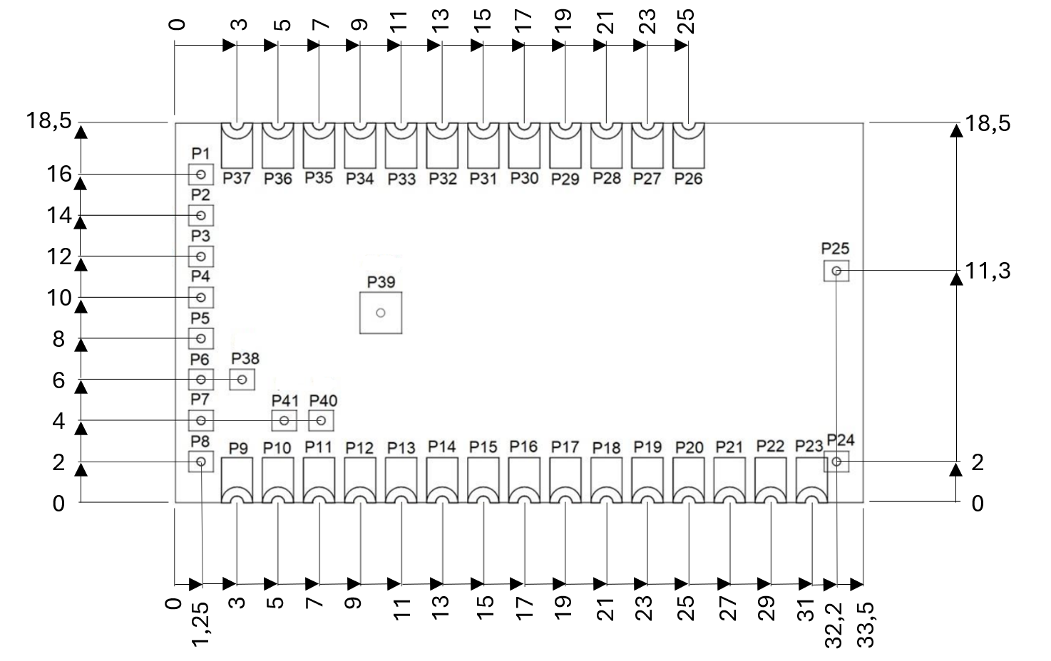
Recommended footprint

- Main pads - oblong 1.4 x 2.79 (oblong edge a half circle with diameter 1.4)
- Small rectangles left edge 1.0 x 0.8 (red)
- Small squares right edge 1.02 x 1.02 (blue)
- Large square 2.0 x 2.0 (green)
Layout considerations for the carrier board
The W-DALI module has been specifically designed to achieve optimal RF performance. To maintain this, we stress the following guidelines:
-
The use of ground planes on the main board cannot be emphasized enough. Good decoupling of any high-speed digital circuitry is a must. Many embedded microprocessors today have clock frequencies with clocks or overtones that reach well into the GHz range. It is perfectly possible for an embedded design to pass any EMC certification and still cause disturbances that will block the RF reception of the W-DALI module. The sensitivity of the W-DALI module receiver is -96 dBm; it is therefore recommended to keep disturbances below -100 dBm in the frequency range of operation.
-
It is essential that all power paths are of low impedance. This means that the power and GND pads must be connected to the source with a sufficient amount of copper (use wide traces and proper via coupling).
-
A near field probe connected to a spectrum analyzer will show if there are any disturbances present on the 2.45 GHz band generated by the microprocessor or any other device that is placed on the main board. Pay special attention to pre-built LAN-products; they pass EMC certifications, but some of them radiate poorly on 2.45 GHz. If disturbances can be seen on a spectrum analyzer - then the W-DALI module will have impaired reception.
-
The W-DALI module has supply voltage decoupling on the circuit board. The supply voltage must still be properly filtered. If interference or intermittent communication failures occur, check the supply voltage for dropouts, switch supply ripple, etc.
-
The TOP layer within the footprint must be free of copper. There is a ground plane on the W-DALI module, but there are also supply lines. It is an unnecessary risk to rely on solder mask lacquer for isolation.
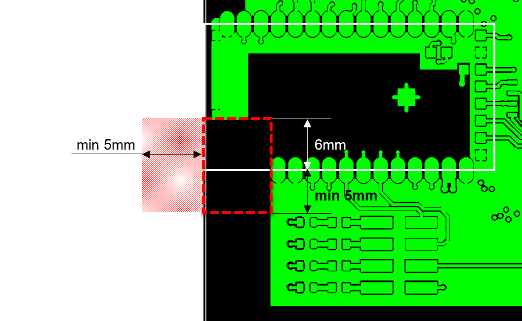
Guidelines for optimal performance of internal antenna
-
The W-DALI module has been tested on 1.6 mm carrier boards of the brands ITEQ IT180 and Isola 370HR. For optimal performance it is recommended to use those for the carrier board design or a PCB with similar specification.
-
A minimum of 5 mm distance to solid objects under and above the W-DALI module antenna area. Note that carrier board thickness can be included in the total distance to solid objects under the antenna. That is, for a 1.6 mm carrier board, standoffs needs to be min 3.4 mm.
- Minimum dimensions for ground plane clearance for optimum antenna performance are shown below:
![]()
- Red diagonal striped area is a keep out area "air gap" from any solid objects
or carrier board PCB material.